Virtual Testing of Integrated Microelectronics
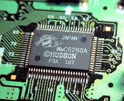
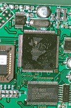
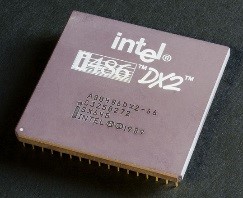
Integrated Circuits (ICs) or packaged microelectronics are terms used to describe components that can be found in nearly every single electronic system in existence. They serve many roles and are referred to specifically by their function, such as: CPUs, GPUs, DSPs, and others. Though difficult to quantify, it is known that they are produced in staggering numbers and have a large impact in the national and global economies. Their volume and diversity create many challenges in quality assurance and the refinement of counterfeiting techniques along with the the huge profit margin that exists among different IC grades produced a thriving and invasive community of counterfeit devices, prone to premature failure. In addition, the advancement of nanofabrication processes has so far made the exponential miniaturization of these systems a reality (according to Moore’s Law). This has the immediate benefit of improved performance but cascades issues related to the mechanical, thermal and overall quality assurance of these increasingly complex systems.
| 10 billion | 164 billion | 20% |
| Estimated number of CPUs manufactured in 2008 – that’s just one type of IC and only the number that were created in one year. Circulation numbers are much harder to track | Contribution of semiconductor sales to the US GDP. That makes it our #4 export. Because of that large contribution, US is responsible for over 50% of global source. | Average percentage of revenue that is reinvested into R&D, nationwide. This is what makes Moore’s Law hold true. |
Within industries that manufacture and/or utilize semiconductor devices, integrated circuits are tested for product assurance and counterfeit detection purposes through invasive and destructive probing. The examined unit is either partially damaged or fully destroyed during these tests and the uncertainties that existed prior to testing reappear when a new unit must replace the probed unit. Because of the aforementioned challenges, there is a strong need for robust, quick, and non-destructive testing. As of now, methods to nondestructively test these components involve either simplified geometric modeling and finite element analyses, which make concessions to accuracy, or include more accurate forms of geometric acquisition but remain untested, unverified, and computationally expensive. The goals of my research are to test the validity of micro-CT as a tool to import accurate bond wire geometries to single- and multi-physical finite element testing and to produce a practical methodology for the image acquisition, processing, and simulation of integrated circuit bond wires with a focus on practicality and industrial applicability. I utilize reverse engineering techniques as a valid simplification to the geometries retrieved from micro-CT. The preliminary results of my finite element model, when compared to the destructive in-situ testing, show that the proposed methodology can reduce finite element computational expense by a factor of four and produce a CAD editable model for geometric alteration and other finite element testing environments; all while closely mirroring the destructive test findings. The broader implications of this methodology include its application to iterative product design and extension to multi-physical, dynamic, and/or inordinately expensive testing conditions.

|
 |
 |